用非補償運放改進性能
 (1)
(1)
![]() (2)
(2)
![]() (3)
(3)
Table 2 shows a small section of the spreadsheet calculations to help you visualize the gain roll-off with frequency. You calculate equation 1, equation 2, and equation 3 versus frequency in columns 1, 2, and 3, respectively (Figure 1).
The next step is to find the frequency at which the gain error is equal to a ½ LSB of an ADC with specified bits of resolution. Equation 4 calculates the ½-LSB error, given the resolution of the ADC (Table 1).
![]() (4)
(4)
To calculate the frequency at which the gain error is equal to the ½-LSB error, substitute Equation 4 into Equation 1 and rearrange it, yielding Equation 5 . You use equation 4 and equation 5 to calculate the values in Table 3.
 (5)
(5)
In Table 3, the column with the heading “Frequency at error” gives the frequency at which the gain error is equal to a ½ LSB of the ADC’s resolution. At lower frequencies, the gain error is less than ½ LSB. This bandwidth is effective for the specified resolution. For example, the effective bandwidth of an amplifier driving a 10-bit ADC is 0.03126 of the –3-dB frequency, and the effective bandwidth of a 14-bit ADC is 0.007813 of the –3-dB frequency. If the amplifier has a closed-loop, –3-dB frequency of 100 kHz, the effective bandwidths are 31.3 and 7.81 kHz, respectively. Equation 1 through Equation 5, which divide the gain bandwidth of an amplifier by its closed-loop gain, demonstrate that an amplifier’s effective bandwidth is substantially less than the –3-dB frequency that the theoretical usage reports.
Considering how you are using an amplifier in the signal path can partially offset the rapid loss of effective bandwidth. Amplifiers commonly use some amount of gain to scale the signal from a sensor to the input of an ADC. In many cases, the gain is greater than 10. Using gain with an amplifier eliminates the need for unity-gain stability and reduces the amount of internal compensation the amplifier uses. The advantage of decompensating the amplifier is an increase in the available bandwidth and slew rate for the same power consumption.
Compensated versus decompensated
National Semiconductor’s LMV793 and LMV796 use the same design except for the amount of internal compensation. The LMV796 is unity-gain-stable, and the LMV793 is decompensated for a gain of 10. Figure 2 plots the open-loop gain on a sample of each amplifier. The LMV796 displays the classic single-pole response with a pole at approximately 60 Hz and a unity-gain-crossover frequency of 17 MHz. The gain plot for the LMV793 shows a two-pole open-loop response due to decompensating, or undercompensating, the amplifier. The plot shows the open-loop-gain shift to the right, indicating the higher frequency response of the LMV793. The first pole occurs at approximately 500 Hz, which is 440 Hz higher than that for the LMV796. A second pole occurs at 45 MHz, and the open-loop gain decreases at –40 dB per decade and crosses the 0-dB axis at approximately 56 MHz. The device achieves this increased bandwidth without an increase in power consumption.
The decompensated LMV793 has significantly more bandwidth for the same current consumption as the fully compensated LMV796. This feature can provide a power savings over using a higher frequency, fully compensated amplifier, which typically would require a higher supply current.
For the LMV793, the gain bandwidth is 88 MHz for closed-loop gains of 10 or more. A second pole occurs before the open-loop gain of 1, at approximately 51 MHz. For decompensated amplifiers, the unity-gain frequency and the gain bandwidth are no longer equal. The LMV793’s minimum gain for stability without using additional external compensation is 10 or 20 dB.
The frequency-dependent closed-loop gain depends on the amplifier’s gain bandwidth. Amplifier data sheets routinely specify the gain bandwidth of an amplifier, and, using the closed-loop gain of the amplifier, you can easily calculate the –3-dB bandwidth. For example, the LMV796 has a gain bandwidth of 17 MHz, and, if the closed-loop gain is 100, the bandwidth of the amplifier is 0.17 MHz, or 170 kHz, and is the –3-dB point in the amplifier’s frequency response. This point also has almost 30% gain error. The decompensated LMV793 has a gain bandwidth of 88 MHz for gains greater than 10. Continuing the example at a closed-loop gain of 100, the LMV793 has a bandwidth of 0.88 MHz, or 880 kHz. The LMV793 has a gain bandwidth of 88 MHz at a gain of 10 and a slew-rate rising edge of 40V/µsec. In contrast, the LMV796 has a gain bandwidth of 17 MHz at a gain of 10 and a slew-rate rising edge of 9.5V/µsec.
Added components affect gain
Many sensor applications have ac-signal components that can extend to tens of kilohertz and require accurate gain over this frequency range to maintain the amplitude accuracy of the signal. To accurately amplify a signal, the design must account for gain errors as a function of frequency. Table 4 shows the results of applying the effective-bandwidth concepts to the LMV793 and LMV796. An LMV796 with a closed-loop gain of 100 and a bandwidth of 170 kHz would have the effective bandwidth that Column 4 of the table shows for the range of resolutions the table lists. For example, at an ADC resolution of 14 bits, the effective bandwidth would be 1328 Hz. Table 4 shows that the LMV793 with a closed-loop gain of 100 and a bandwidth of 880 kHz would have the effective bandwidth that Column 5 lists for the range of resolutions the table lists. This amplifier, at an ADC resolution of 14 bits, has an effective bandwidth of 6875 Hz. As this example shows, the effective bandwidth is a small fraction of the –3-dB bandwidth.
A decompensated amplifier offers substantially more effective bandwidth for the same power consumption and gives the designer an additional degree of freedom in amplifier selection. The decompensated amplifier offers additional bandwidth that can support higher ADC resolutions.
In discussions about the closed-loop bandwidth of amplifiers, engineers often apply the gain bandwidth to noninverting and inverting amplifiers to estimate the closed-loop bandwidth. Equation 6 relates the closed-loop bandwidth to the amplifier’s gain bandwidth and closed-loop gain.
![]() (6)
(6)
where BW is the bandwidth and GBW is the gain bandwidth.
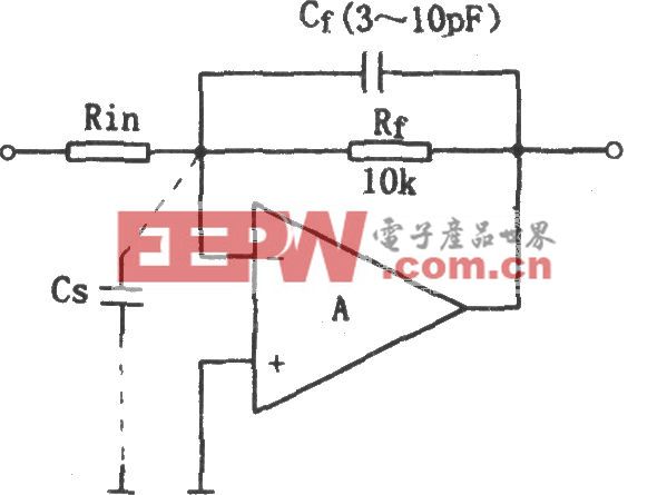
The equation expresses a relationship that applies to noninverting amplifiers and approximately to inverting amplifiers. As the gain of the inverting amplifier increases, the error in bandwidth, using Equation 6, becomes smaller. This consideration is important when you are using different amplifier configurations. Figure 3 shows configurations of basic inverting and noninverting amplifiers.
Consider beta
The closed-loop bandwidth of an amplifier is a function of the gain and the amount of feedback, also known as the feedback factor, beta. Beta is the portion of the amplifier’s output that feeds back to the input. You calculate the beta of both configurations with the following equation:
![]() (7)
(7)
The beta differs for noninverting and inverting amplifiers with the same absolute value of gain due to the difference in the resistor ratios necessary to set the same absolute value of gain. Table 5 shows the calculated beta and normalized bandwidth for gains as high as 10 and –10. Equation 8 shows the calculation for the bandwidth of a unity-gain-stable amplifier in the inverting or the noninverting configuration:
![]() (8)
(8)
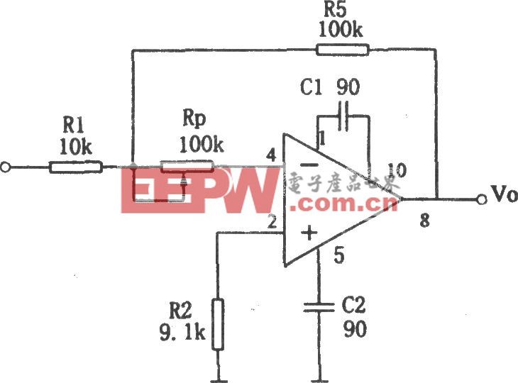
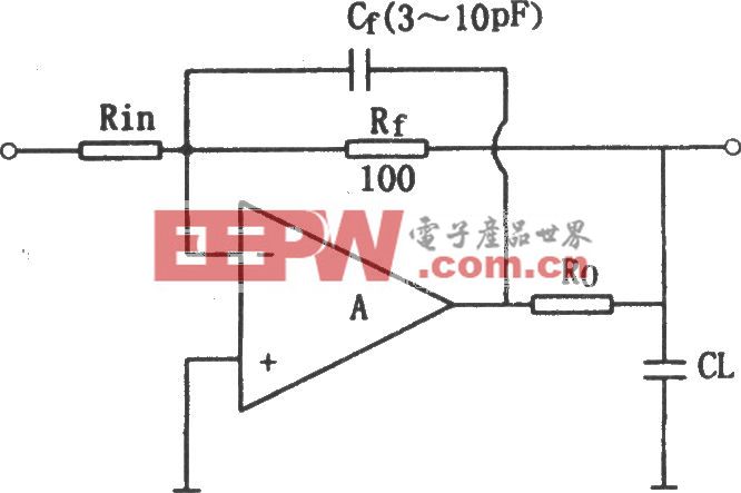
Figure 4 shows the bandwidth-versus-gain relationship, demonstrating that, at low gains, there is significant loss of closed-loop bandwidth for the inverting amplifier. For example, the bandwidth of the inverting amplifier with a gain of –1 is half the bandwidth of the noninverting amplifier with a gain of 1. In these cases, if an application requires additional bandwidth at the same level of power consumption, using a decompensated amplifier is an acceptable alternative. Offsetting the additional bandwidth at lower gains is the required external compensation to prevent the amplifier from oscillating. Figure 4 also shows the bandwidth of the inverting gain to be asymptotic to the noninverting gain as the closed-loop gain increases. To externally compensate the decompensated amplifier for low gains, refer to the LMV793 data sheet, which details various compensation techniques.
In summary, decompensated amplifiers provide an additional degree of freedom to circuit designers in meeting the performance, power, and price targets of their design. The additional circuitry that may be necessary for external compensation has little effect on overall complexity but allows a more customized design to give better overall performance. Regardless of which design you use, understanding the details and trade-offs is necessary to fully meet the required specifications.




評論