能源管理的小型便攜式系統(tǒng)-Energy Management

Numerous diverse and conflicting constraints burden the designer of small hand-held products. Aside from the customary restrictions on size and weight, these constraints include cost limitations, strict time schedules, battery-life goals measured in weeks instead of hours, and host computers that are (sometimes) overtaxed with the demands of power management.
Because power requirements for hand-held applications vary widely with product use, no single "best" power source exists for these applications. A device used intermittently is more concerned with no-load quiescent current than with full-load efficiency, and so may operate satisfactorily with alkaline batteries. Cell phones, on the other hand, must contend with high peak loads and frequent use. This mode of operation emphasizes conversion efficiency over quiescent current, so cell phones are better served with a rechargeable battery.
In hand-held product design, size limitations often dictate the number of battery cells early in the process. This is frustrating to the electrical engineer, and a substantial constraint, since the number (and type) of cells allowed determines the operating-voltage range, which in turn strongly affects the cost and complexity of the power supply. High cell counts enable the use of linear regulators and simple circuitry at the cost of extra weight and limited efficiency. Low cell counts compel the use of a more costly switching regulator, but the low cost of the battery may justify this expense.
Four-Cell Designs
Four-cell batteries often provide an attractive compromise between weight and operating life. That number is particularly popular for alkaline batteries because they are commonly sold in multiples of four. Four-cell power for 5V circuitry presents a design challenge, however. As the battery discharges, the regulator must first step down, and then step up. This requirement precludes use of the simpler, one-function regulator topologies that can only step down, step up, or invert.
One effective solution to this problem is the SEPIC (single-ended primary inductance converter), in which VOUT is capacitively coupled to the switching circuitry (Figure 1). The absence of a transformer is one of several advantages this configuration has over flyback-transformer regulators and combination step-up/linear regulators.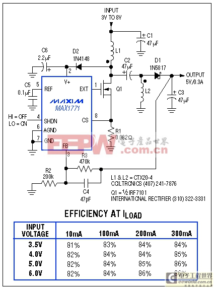
Figure 1. This regulator topology supplies 5V for inputs ranging from 3V to 8V. The operation shifts smoothly between step-up and step-down conversion without steps or mode changes. During shutdown, the output turns off completely and sources no current.
As another improvement over boost designs (in which current drains from the battery during shutdown unless you add a cut-off switch—see (Figure 2), the SEPIC output fully turns off in response to a shutdown command. As VIN falls during normal operation, the SEPIC circuit smoothly regulates VOUT without shifting its mode of operation as VOUT approaches VIN. Its power-conversion efficiency peaks at 86%, near 200mA (Figure 1).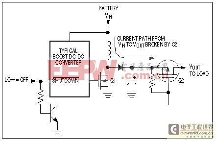
Figure 2. Typical dc-dc boost converters provide a current path from input to output, even when powered down. To interrupt this path, you must add a disconnect switch (Q2).
Coils L1 and L2 (Figure 1) should be the same type and have the same value, but coupling between them is not required. They can be wound on the same core for convenience, but the circuit works equally well if they are completely separate. Each coil passes only one half of the peak switching current (IPEAK = 100mV/R1 = 1.22A), so each can be rated accordingly.
Capacitor C2 couples energy to the output and requires low ESR to handle high ripple currents. A low-ESR Sanyo OS-CON capacitor, for instance, offers 3% more efficiency than does a less expensive 1μF ceramic capacitor. Tantalum capacitors are not recommended because high ESR causes them to self-heat at high ripple currents.
Diode D2 provides a supply voltage for the IC (pin 2) by capturing switching pulses at the drain of Q1. Although this voltage (approximately the sum of VIN and VOUT) limits the maximum VIN to 8V, it improves the start-up capability under full load and improves the low-VIN efficiency by boosting gate drive to the external MOSFET. If VIN does not fall below 4V, you can substitute a 3V-threshold FET for Q1 and omit D2. In that case, pin 2 connects directly to VIN, which assumes an upper limit of 16.5V.
Three Cells to 3.3V
The circuit of Figure 3 employs the same principles as that of Figure 2, but adds battery-backup capability. It also foregoes the external FET for a lower-current internal one. Separate coils for L1 and L2 (vs. a single transformer) allow the use of a 22μH coil for each of multiple versions of the circuit—such as you would need in a product that required power supplies of 3.3V, 5V, 12V, and 30V, for example. The input-voltage range is 3V to 13V.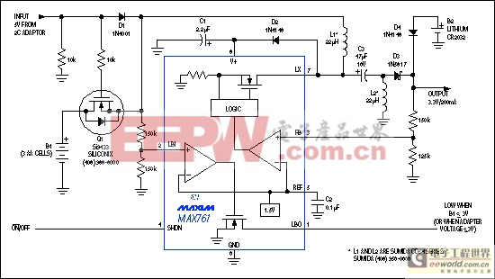
Figure 3. This low-current step-up/step-down regulator supplies 3.3V at 200mA. Q1 automatically disconnects the B1 battery when you connect an ac adapter, and a diode-OR circuit allows B2 to back-up the 3.3V output.
During normal operation, the ac adapter's 5V output powers the circuit and turns off Q1. Disconnecting the adapter removes 5V, turns on Q1, and allows the three AA cells to provide power. If the input voltage drops below 3.0V, a low-battery comparator in IC1 alerts the system by driving LBO low. And for backup, a diode-OR connection allows the optional lithium battery (coin cell B2) to maintain the 3.3V output. To simplify the switchover circuit from adapter to main battery, this design requires the ac adapter's 5V output to be somewhat regulated—to between 4V and 5.5V.
Low-Dropout, Step-Down Converter
Low-voltage logic, such as that powered from 3.3V, now enables the use of 4-cell inputs for simple step-down configurations that optimize efficiency and cost. For 3.3V outputs, the key specification is dropout voltage—the minimum allowable difference between VIN and VOUT. "End-of-life" voltage for the battery varies according to cell type and the product's pattern of use, but (for all but lithium batteries) it falls in the range of 0.8V to 1V per cell. As a result, it's not uncommon for 3.3V regulators to operate with input voltages as low as 3.6V.
The design of Figure 4 offers an uncomplicated means for delivering intermediate current loads at 3.3V from four cells. The IC drives a low-threshold p-channel MOSFET, and minimizes current-sense losses with a low current-sense voltage of 110mV. For best performance, the MOSFET on-resistance should be specified in conjunction with the circuit's lowest operating voltage—about 3.6V in this case.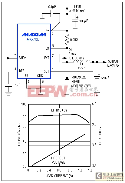
Figure 4. A low-dropout switch-mode controller and p-channel MOSFET supply 3.3V at 1.5A with inputs as low as 3.8V. Efficiency exceeds 90% for most of the operating range.
Linear Regulators
Still the lowest-cost approach for many step-down applications (short of no regulator at all) is linear regulation, provided its efficiency and battery-life limitations are acceptable, and its power dissipation at higher VIN is manageable.
For portable designs, even a simple linear regulator can provide some twists. As an example, dropout voltage (the low-VIN level at which output regulation is lost) should often be regarded as a part of normal operation rather than a fault. That is, to extend operating time it may be advisable to allow the regulator to fall out of regulation without shutting down. The regulator's behavior during dropout (especially its quiescent current) is important in these designs.
The simple linear regulator of Figure 5 offers exceptional dropout behavior with little effect on operating current. Essentially an 8-pin surface-mount package, it delivers more than 400mA. Because the internal pass element is a MOSFET instead of a bipolar transistor, the circuit's dropout voltage is nearly zero at light loads. And, its quiescent current does not rise as VIN approaches VOUT.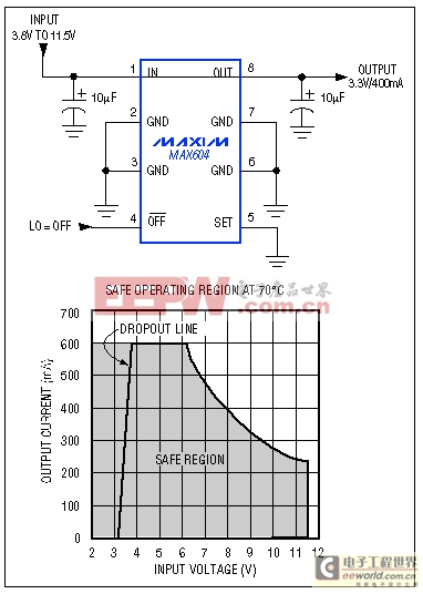
Figure 5. This combination of internal MOSFET pass transistor and high-power SO-8 package provides a linear regulator with low dropout, an operating current of 15μA, and an output capability of over 400mA.
This last characteristic is especially important for small portables whose steady-state load is no greater than 100μA. In such designs, the milliamp or more of quiescent-current rise (typical of a low-dropout regulator with bipolar pass transistor) accelerates the battery discharge at a time when the battery can least afford it: near the end. Typically, the IC in Figure 5 draws 15μA of operating current whether in or out of dropout.
Boosting from Low-Cell-Count Batteries
The cell count for batteries in earlier-generation designs was high—not to provide more energy, but rather to allow generation of the system voltages with low-cost linear regulators (or even with no regulator at all). The latest generation of voltage-conversion ICs, on the other hand, lets you reduce the cell count while adding a minimum number of external parts. Usually, this extra cost is more than offset by the benefits of lower cell count: smaller size, less weight, and (sometimes) longer battery life. To illustrate, the 4.5Whrs of available energy in two AA cells exceeds the 3Whrs in a 6-cell, 9V alkaline battery by 50%, even though the two batteries are comparable in size and weight.
The step-up regulator of Figure 6a provides high, 88% efficiency for 2-cell and 1-cell inputs, and its high, 500kHz switching frequency enables the use of very small inductors. The IC's quiescent current is only 60μA at light or zero loads—an attractive feature for portable products whose supply voltage must remain active when the product is turned "off." As the product enters such an idle or suspend mode, load current falls to microamps and must not be dominated by current into the regulator IC. For equipment that truly shuts down, the IC provides a very low-current shutdown mode in which it draws less than 1μA.
One-Cell Regulators
It makes sense to operate from a 1-cell battery when size is of prime importance. Reasonable efficiency and cost is now possible when operating with inputs below one volt, so many hand-held applications have become new candidates for 1-cell operation. The switching frequency for low-cost ICs now approaches 1MHz, which permits the use of small magnetic components available from multiple sources. It's not unusual, therefore, for the dc-dc circuitry to occupy less space than the battery it replaced.
In Figure 6a, the addition of Q1 and Q2 within the dashed lines allows the regulator to start with lower input voltages and higher load currents. Q1 also disconnects the load and battery from each other during shutdown, and the on-chip comparator does not allow Q1 to turn on again until VOUT has risen to at least 3V. Figure 6b illustrates this circuit's loaded-start capability and its remarkably low typical start-up voltage (0.8V).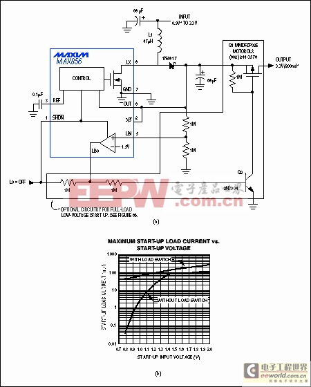
Figure 6. This low-power, CMOS step-up converter (a) generates 3.3V from 1-cell and 2-cell inputs. The optional load-disconnect circuitry (dashed lines) enables the circuit to start with inputs as low as 0.8V (b).
Figure 7 shows a low-parts-count step-up regulator that also starts under load and operates with inputs down to 0.8V. Its 500kHz switching frequency and adjustable peak coil current (set by RLIM) allows use of a tiny, low-cost surface-mount coil. The on-board active (synchronous) rectifier not only eliminates the external diode, it also enables the shutdown input to turn off the output completely—a useful feature not common in boost designs, and one that requires an external FET in Figure 6.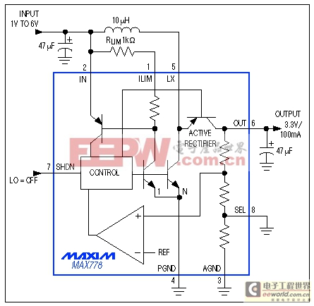
Figure 7. This single-IC boost converter has an internal synchronous rectifier. It maintains a regulated 3.3V output for inputs ranging from 1V to 6V.
The active rectifier and control circuitry in the IC of Figure 7 maintain regulation for inputs to 6.2V—an achievement which, if not of benefit in single-cell designs, may be useful elsewhere. The price for these improvements is higher quiescent current: 190μA for Figure 7 vs. 30μA for Figure 6.
Inductorless Conversion Suits Tight Spaces
Despite the advances made in inductor-based switching regulators, most designers would regard the ideal converter circuit as one that has no inductor. The capacitor-based alternatives (charge-pump converters) were hampered in the past by their lack of regulation and limited output current. Though still low compared to that of switching regulators, their output current is now adequate for many designs. And in some cases, the charge-pump advantages are compelling—low cost, small size, and reduced EMI. Charge pumps are particularly useful in PCMCIA systems and other "credit-card" products in which the component height is limited.
Figures 8, 9, and 10 illustrate three inductorless voltage converters. In Figure 8, the output of a 2-cell battery or other low-voltage source is converted to a regulated 5V ±4%. The IC changes its operational mode with input voltage, producing a tripler at low VIN, a doubler at high VIN, and a tripler-doubler at mid-range that changes modes every switching cycle. Efficiency ranges from 85% to 65%. Low supply current—typically 75μA for no-load operating conditions and 1μA in shutdown—makes the circuit useful as a coin-cell-powered backup supply for DRAM or PSRAM.
Figure 8. With a few external capacitors, one IC boosts a 2-cell or 3-cell input to 5V, and delivers 50mA (for 3V inputs) with only 75μA of quiescent current. With an additional SOT-23 dual diode and two capacitors, it also produces a small negative output.
The optional diode-capacitor network in Figure 8 generates an unregulated negative voltage between -1.4V and -3V. Acting as a negative supply, this output simplifies analog designs by allowing the use of inexpensive op amps. The negative rail assures that such op amps can swing completely to ground.
Another charge-pump circuit, built in less than 0.1in.2 of board area, converts 5V to the 12V level required for programming "flash" memory chips (Figure 9). Common in PCMCIA cards, flash memory is popular for compact portable applications because it provides large amounts of nonvolatile storage in a small space, and because it needs power only for read and write operations. Some flash ICs operate on 5V, but those with the highest memory densities require 12V for programming.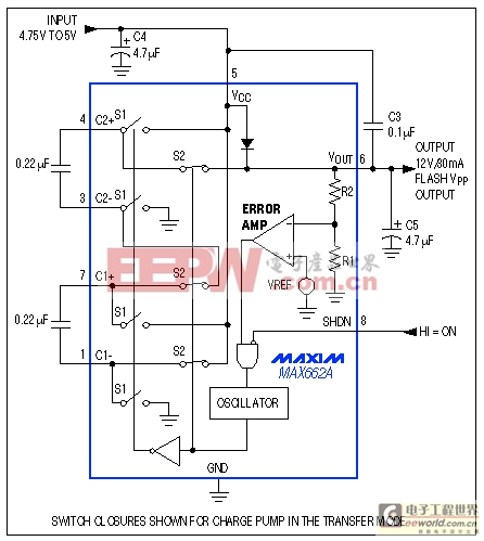
Figure 9. For programming flash memory, this circuit generates a regulated 12V/30mA programming voltage without inductors. It's small enough to fit into "smart cards" the size of a credit card.
A third application that benefits from the use of charge pumps is the optimization of RF-transmitter efficiency in cellular and other voice/data wireless transceivers. "Talk time" in these transceivers is extended by the use of power amplifiers based on gallium-arsenide FETs (GaAsFETs), which are more efficient than those based on bipolar transistors.
Though more efficient, a GaAsFET costs more and requires a small negative bias voltage. Typical charge pumps generate too much noise for this application, but an output voltage regulator in the chip of Figure 10 holds the output noise and ripple to 1mVp-p. Tying the FB terminal to ground sets the regulated output to -4.1V (you can set other output levels with two external resistors). Regulation and low noise are achieved with an output linear regulator—unlike the circuits of Figures 8 and 9, which regulate by gating the charge pump's switching action.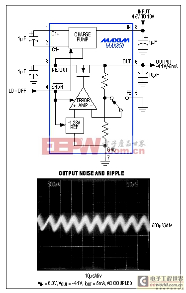
Figure 10. Intended for biasing efficient GaAsFET RF power amplifiers, this charge-pump voltage inverter includes a super-quiet linear regulator that limits output ripple and noise below 1mVp-p.
Intermittent High-Current Loads
A second requirement in many hand-held wireless designs is a quick response to abrupt load changes. The power supply may idle at milliamp levels for most of the time, but to handle short RF transmissions or bursts of CPU activity it must also deliver high-amplitude currents for short intervals. Especially demanding is the RF transmitter in a GSM cellular telephone or other digital wireless system employing TDMA (time-division multiple access) techniques.
For cellular handsets, a desirable battery combination for minimal size and weight is three NiCd cells. The lowest-cost RF transmitters for this application operate at or near 6V. You might expect the expense of a switching regulator capable of delivering 2W at 6V to force the use of a five-cell battery. But, the high current is drawn only for 600μs or so at a 10% duty cycle, so a small step-up IC can supply the load.
In Figure 11, a reservoir capacitor powers both the TDMA logic and the RF circuitry. The capacitor supplies an average 200mA, but at 1.5A its output drop is less than 500mV after 577μs. A 1Ω resistor (R1) isolates the RF load from the dc-dc converter IC. While 4 x 470μF is certainly a lot of buffer capacitance in a hand-held device, the four surface-mount capacitors are far smaller and cheaper than two additional battery cells. The circuit's average power-conversion efficiency is 80%, and its quiescent supply current is only 60μA.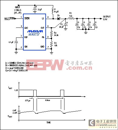
Figure 11. This circuit includes a large capacitive reservoir that supplies 1.5A transient loads in a GSM cellular telephone. The average load is only 200mA, so the 8-pin, surface-mount, boost-regulator IC requires no external MOSFET.
LCD Bias Supplies
The bias requirements for LCD panels in portable gear cover broad ranges of voltage and current, depending on the display's technology, screen size, and cost. Bias voltages may be positive or negative and as high as ±30V. The boost converter in Figure 12, for example, produces an output range of 20V to 30V, adjusted either by digital control or by an external potentiometer. This circuit's high switching frequency and adjustable inductor-current limit enable the use of small surface-mount inductors and output-filter capacitors. For loads below 10mA, for instance, the Murata-Erie LQH4 coil shown is only 2.6mm high.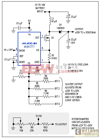
Figure 12. This circuit produces a bias (contrast) voltage for LCD panels that can be adjusted either with a potentiometer or digitally with a 4-bit homemade D/A converter.
Note that the potentiometer's configuration is not arbitrary (see the optional circuit in Figure 12). Connecting the pot between FB and ground (rather than FB and VOUT) ensures that an open or noisy pot wiper will produce a low output voltage rather than a maximum (and possibly destructive) output. Moreover, connecting the pot and its wiper to ground minimizes the trace area at FB; if you swap R8 and R9 the VOUT noise will likely increase.
In 2- or 3-cell applications you can optimize efficiency by biasing the IC from 5V (if available) instead of the battery voltage. The inductor still draws current from the battery, but higher voltage at the chip's V+ pin improves efficiency by providing more gate drive to Q1, which lowers its on-resistance. On the other hand, if battery voltage exceeds 5V then V+ should connect directly to the battery. VOUT can be adjusted by a 4-bit, 3.3V CMOS digital code or by the optional potentiometer, as shown.
Multiple Supply Voltages
Many portable designs require more than one supply voltage. Even as IC manufacturers add to the list of functions that can be powered from standard 3.3V and 5V levels, the need to optimize performance, weight, battery life, and cost continues to justify additional voltages. Fortunately, the use of multi-output ICs minimizes the number of components needed to create these voltages. These ICs minimize the board area and the number of "glue" components required, while improving the system's low-load efficiency and other performance parameters.
With two ICs you can design a four-output power supply for hand-held organizers, computers, or data terminals (Figure 13). The output voltages are 5V for PCMCIA slots and analog circuitry, 3.3V for CPU and RAM, 12V for flash memory, and -17V for LCD backplane bias.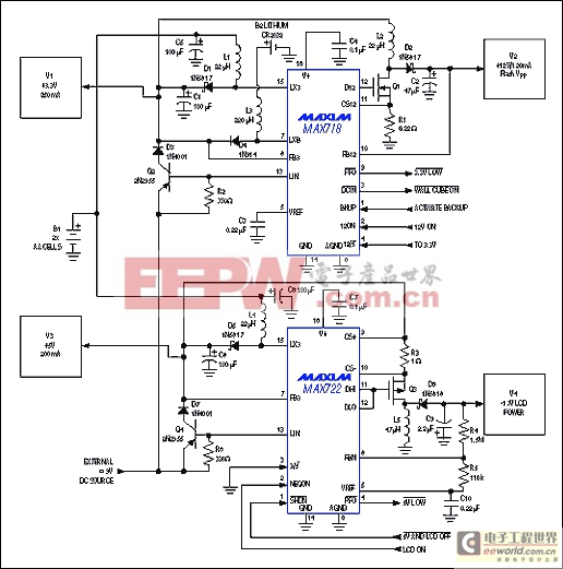
Figure 13. These two ICs perform a multitude of power-related tasks in a system powered by two AA cells. They generate four supply voltages, supervise the system power, control a lithium backup battery, and provide a switchover between battery and wall-adapter outputs.
A fifth regulator—a micropower boost circuit—is included for backup during battery replacement. It sits idle until the main battery dies or is removed, then supports the 3.3V rail by boosting the output of a lithium coin cell. The 5V and 3.3V main outputs are also overridden by pnp linear regulators (Q2 and Q4), which become active when you plug in an external unregulated dc supply. This action also unloads the main battery. The two ICs include several control and supervisory lines in addition to the four output voltages.
Simple Battery Charging
For small hand-held products, a lack of space and a limited budget often preclude sophisticated schemes for battery monitoring and charging. The goal in these cases is to squeeze the maximum performance from "bare bones" hardware. If available, though, CPU resources (combined with low-cost analog circuitry) offer a convenient means for charge control.
The 8-pin, step-down, switching regulator IC of Figure 14 is configured as a high-efficiency 1A current source, activated via a logic-level signal. The op amp (IC2) monitors the charging current with a sense resistor (R10) and applies feedback to the regulator chip. This "high side" current sensing lets the negative battery terminal connect directly to ground.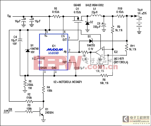
Figure 14. This 1A switch-mode current source supplies charging current to a grounded battery by sensing current on the "high side." An op amp senses the output current and supplies feedback to the dc-dc converter IC.
Switch-mode battery charging offers advantages, even for low-cost applications; it dissipates less power and makes full use of an ac adapter as a power source. Linear-regulator designs typically require wall cubes with twice the power rating, after you consider high- and low-amplitude extremes for the ac-line voltage. Linear designs also require heatsinks to implement fast charging.
The circuit shown generates a regulated current for charging a 3-cell battery. A 5.1V zener diode (D3) clamps the output at approximately 6.3V when the battery is removed. You can adjust for other battery voltages and currents by changing R5, R10, and D3. The operating-voltage range is 5V to 16V, but surges to 24V are allowed (with some output error).
If a fast charge is desired but no CPU resources are available, an "all-in-one" controller may solve the problem (Figure 15). IC1 is a low-cost NiCd charge controller operating in a low-loss, switch-mode charging configuration. The DRV pin drives a p-channel MOSFET (Q1) via the bipolar-transistor buffer Q1-Q2. The cell count (2 to 16), charge rate, and trickle-charge current are pin programmed via the IC's PGM0-PGM3 inputs.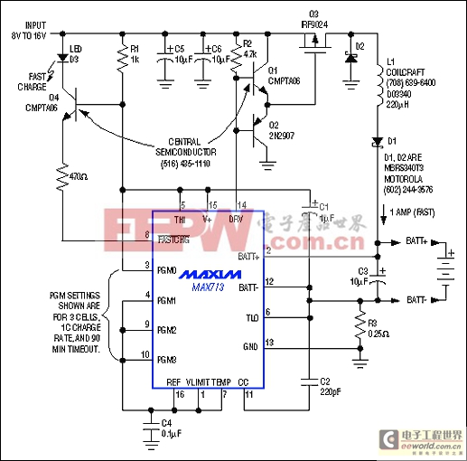
Figure 15. A low-cost battery-charge controller is the heart of a low-dissipation, fast-charge switch-mode circuit. When the battery is fully charged, the circuit shifts automatically to a C/16 trickle charge.
The circuit terminates a fast charge automatically by detecting a negative slope in the curve of battery voltage vs. time. For safety, it also provides an adjustable timeout as backup for terminating the charge. Note that NiMH batteries require termination at zero slope rather than negative slope. For NiMH batteries, replace the MAX713 with the pin-compatible MAX712.
Figure 15 accommodates nominal 12V inputs such as a car battery, and is therefore limited to charging batteries of six cells or less. As shown, the PGM0-PGM3 connections set the fast-charge rate at one ampere and the trickle-charge rate at 1/16 of that. The backup timer is set for 90 minutes.


評論