<meter id="pryje"><nav id="pryje"><delect id="pryje"></delect></nav></meter>
          <label id="pryje"></label>

          新聞中心

          EEPW首頁 > 模擬技術(shù) > 設(shè)計(jì)應(yīng)用 > 優(yōu)化音頻橋系桿負(fù)載放大器-Optimizing Audio

          優(yōu)化音頻橋系桿負(fù)載放大器-Optimizing Audio

          作者: 時(shí)間:2011-04-21 來源:網(wǎng)絡(luò) 收藏
          This audio bridge-tied load (BTL) amplifier application note describes a unique architecture that minimizes the differential output distortion and noise (THD+N).


          Low-voltage systems driving loudspeakers often employ a bridged-amplifier configuration that effectively doubles the voltage swing at the transducer (speaker). In a typical bridge-amplifier circuit (Figure 1), an AC-coupled inverting stage with gain drives one side of the speaker. It also drives a second unity-gain inverting amplifier, which drives the other side of the speaker.

          優(yōu)化音頻橋系桿負(fù)載放大器-Optimizing Audio
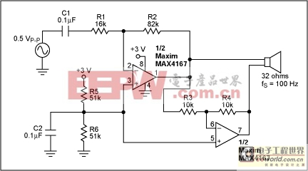
          Figure 1. This conventional bridged amplifier features two amplifiers in tandem.

          Bridged amplifiers usually incorporate a matched pair of amplifiers, but the first amplifier dominates overall performance because its output noise and distortion are replicated in the second amplifier. You can eliminate this drawback by placing the two amplifiers in a non-cascaded configuration, in which one is inverting and the other in non-inverting (Figure 2). Both amplify the same input signal, so neither one reproduces noise, distortion, or clipping introduced by the other.

          優(yōu)化音頻橋系桿負(fù)載放大器-Optimizing Audio
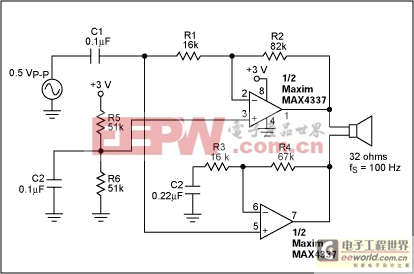
          Figure 2. This circuit optimizes the Figure 1 configuration by apportioning gain between the two amplifiers.

          As a key improvement in Figure 2, DC bias for the non-inverting circuit is derived from the inverting amplifier's source resistor. (Bias is required because the input is AC coupled). Using the other amplifier's source resistor as a bias source lowers the component count and eliminates signal injection into the high-impedance bias source (VCC/2, applied to the top amplifier's non-inverting input).

          Another advantage in Figure 2 is the elimination of DC gain in the non-inverting amplifier. For the circuit shown, C2 sets the -3dB point at half the input cutoff frequency, and R1/C1 sets the input highpass cutoff frequency at 100Hz.

          A similar version of this article appeared in the November 19, 2001 issue of Electronic Design magazine.


          評(píng)論


          相關(guān)推薦

          技術(shù)專區(qū)

          關(guān)閉
          看屁屁www成人影院,亚洲人妻成人图片,亚洲精品成人午夜在线,日韩在线 欧美成人 (function(){ var bp = document.createElement('script'); var curProtocol = window.location.protocol.split(':')[0]; if (curProtocol === 'https') { bp.src = 'https://zz.bdstatic.com/linksubmit/push.js'; } else { bp.src = 'http://push.zhanzhang.baidu.com/push.js'; } var s = document.getElementsByTagName("script")[0]; s.parentNode.insertBefore(bp, s); })();