ADIAD578018位精度低噪音±10VDC電壓源解決方案

The AD57801 is a true 18-bit, unbuffered voltage output DAC that operates from a bipolar supply of up to 33 V. The AD5780 accepts a positive reference input range of 5 V to VDD ? 2.5 V and a negative reference input range of VSS + 2.5 V to 0 V. Both reference inputs are buffered on chip and external buffers are not required. The AD5780 offers a relative accuracy specifica-tion of ±1 LSB maximum range, and operation is guaranteed monotonic with a ±1 LSB DNL maximum range specification.
The part uses a versatile 3-wire serial interface that operates at clock rates of up to 35 MHz and is compatible with standard SPI, QSPI?, MICROWIRE?, and DSP interface standards. The part incorporates a power-on reset circuit that ensures that the DAC output powers up to 0 V in a known output impedance state and remains in this state until a valid write to the device takes place. The part provides an output clamp feature that places the output in a defined load state.
AD57801產(chǎn)品亮點(diǎn):
True 18-bit accuracy.
Wide power supply range of up to ±16.5 V.
?40℃ to +125℃ operating temperature range.
Low 8 nV/√Hz noise.
Low ±0.018 ppm/℃ gain error temperature coefficient
AD57801主要特性:
True 18-bit voltage output DAC, ±1 LSB INL
8 nV/√Hz output noise spectral density
0.025 LSB long-term linearity error stability
±0.018 ppm/°C gain error temperature coefficient
2.5 μs output voltage settling time
3.5 nV-sec midscale glitch impulse
Integrated precision reference buffers
Operating temperature range: ?40℃ to +125℃
4 mm × 5 mm LFCSP package
Wide power supply range of up to ±16.5 V
35 MHz Schmitt triggered digital interface
1.8 V-compatible digital interface
AD57801應(yīng)用:
Medical instrumentation
Test and measurement
Industrial control
Scientific and aerospace instrumentation
Data acquisition systems
Digital gain and offset adjustment
Power supply control
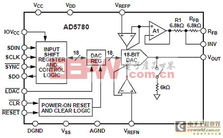
圖1.AD57801功能框圖
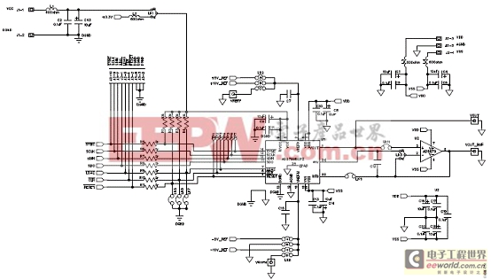
圖2.AD57801典型工作電路圖
AD57801評(píng)估板EVAL-AD5780
Evaluation Board for a 18-Bit Serial Input, Voltage Output DAC with Integrated Precision Reference Buffer Amplifiers
The EVAL-AD5780 is a full-featured evaluation board, designed to allow the user to easily evaluate all features of the AD5780 voltage output, 18-bit digital-to-analog converter (DAC). The AD5780 pins are accessible at on-board connectors for external connection. The board can be controlled by two means: via the on-board connector (J3), or via the system development platform connector (J4). The SDP board allows the evaluation board to be controlled through the USB port of a Windows? XP- (SP2 or later) or Vista-based (32-bit) PC using the AD5780 evaluation software.
評(píng)估板EVAL-AD5780主要特性:
Full-featured evaluation board for the AD5780
Link options
PC control in conjunction with Analog Devices, Inc., system development platform
PC software for control
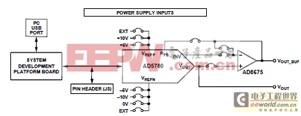
圖3.評(píng)估板EVAL-AD5780框圖
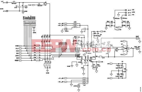
圖4.評(píng)估板EVAL-AD5780電路圖:AD5780
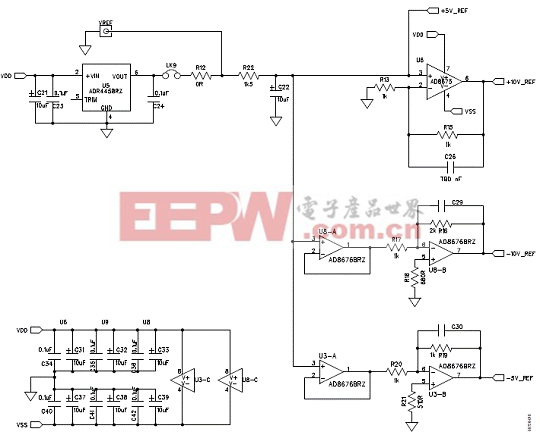
圖5.評(píng)估板EVAL-AD5780電路圖:電壓參考電路
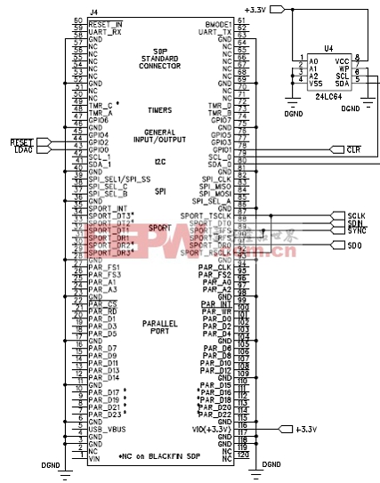
圖6.評(píng)估板EVAL-AD5780電路圖:SDP板連接器

圖7. 18位精度±10V電壓源簡(jiǎn)化電路圖
評(píng)估板EVAL-AD5780材料清單:
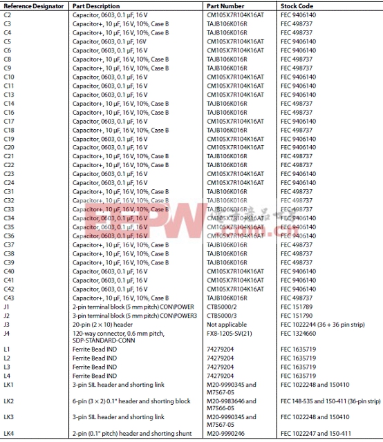
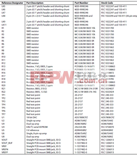
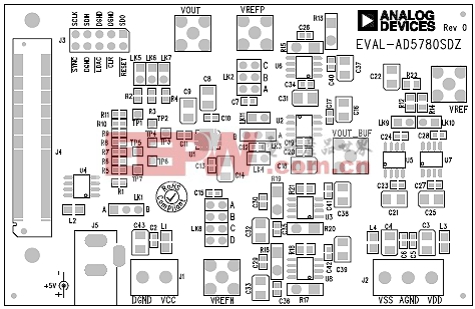
圖8.評(píng)估板EVAL-AD5780 PCB布局圖
詳情請(qǐng)見(jiàn):
http://www.analog.com/static/imported-files/data_sheets/AD5780.pdf
和
http://www.analog.com/static/imported-files/user_guides/UG-256.pdf

電路圖符號(hào)相關(guān)文章:電路圖符號(hào)大全


評(píng)論