視頻解碼器ADV7181B:硬件和軟件設(shè)計(jì)要點(diǎn)
Sample Script
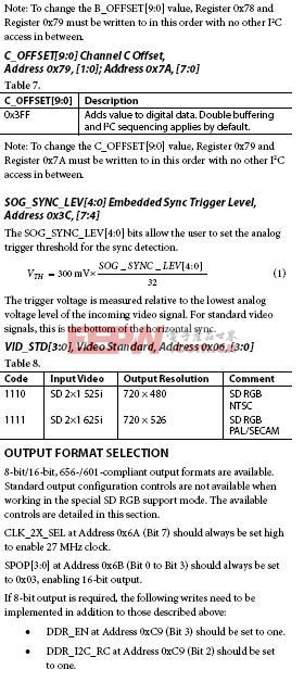
ADV7181B SCART RGB 8-bit 422 out (625i) using 28.6363 MHz Xtal
42 01 88; Disable HS PLL, providing faster response for high quality timebase inputs
42 05 00; Enable the special SD RGB processing block
42 06 0F; Set the input standard for 625i with 2× input oversampling
42 1D 40; Enable 28 MHz crystal
42 0F 40; TRAQ (reset the internal timing blocks)
42 31 02; Clear NEWAV_MODE, SAV/EAV to suit ADV video encoders (only required when back-to-back with encoder)
42 3A 10; Set latch clock (optimized ADC latch clock setting for special mode)
42 3D C3; MWE enable manual window (allow manual control of the blank and burst sample windows)
42 3F E4; BGB to 36 (adjust the sampling window for blank and burst)
42 52 00; Enable the special mode color space converter
42 53 00; Convert from SD RGB to SD YPrPb
42 54 07; Convert from SD RGB to SD YPrPb
42 55 0C; Convert from SD RGB to SD YPrPb
42 56 94; Convert from SD RGB to SD YPrPb
42 57 89; Convert from SD RGB to SD YPrPb
42 58 48; Convert from SD RGB to SD YPrPb
42 59 08; Convert from SD RGB to SD YPrPb
42 5A 00; Convert from SD RGB to SD YPrPb
42 5B 7A; Convert from SD RGB to SD YPrPb
42 5C E1; Convert from SD RGB to SD YPrPb
42 5D 00; Convert from SD RGB to SD YPrPb
42 5E 19; Convert from SD RGB to SD YPrPb
42 5F 48; Convert from SD RGB to SD YPrPb
42 60 08; Convert from SD RGB to SD YPrPb
42 61 00; Convert from SD RGB to SD YPrPb
42 62 20; Convert from SD RGB to SD YPrPb
42 63 03; Convert from SD RGB to SD YPrPb
42 64 A9; Convert from SD RGB to SD YPrPb
42 65 1A; Convert from SD RGB to SD YPrPb
42 66 B8; Convert from SD RGB to SD YPrPb
42 67 03; Convert from SD RGB to SD YPrPb
42 68 00; Convert from SD RGB to SD YPrPb
42 6A 80; Enable 27 MHz LLC output
42 6B C3; Select the 8-bit YPrPb from the special mode output formatter
42 73 D0; Manual gain control
42 74 B4; GAIN setting
42 7B 06; Special mode write to ensure 656 compliant SAV/EAV codes
42 C3 C9; Mux AIN1 to ADC0; mux AIN3 to ADC1
42 C4 8D; Set adc_sw_man_en to 1, mux AIN5 to ADC2
42 85 1A; Enable the sync input mode on Pin 50
42 86 02; Enable the internal special mode sync slicer block
42 B3 FE; SCART RGB write
42 C9 0C; Enable DDR Mode, enable DDR_I2C_RC_First (writing this sequence ensures a 27 MHz output clock)
42 0E 80; Enable design block tweak mode
42 58 ED; Internal timing optimization, not user adjustable
42 90 C9; Internal timing optimization, not user adjustable
42 91 40; internal timing optimization, not user adjustable
42 92 3C; Internal timing optimization, not user adjustable
42 93 CA; Internal timing optimization, not user adjustable
42 94 D5; Internal timing optimization, not user adjustable
42 CF 7C; Internal timing optimization, not user adjustable
42 D0 4E; Internal timing optimization, not user adjustable
42 D6 DD; Internal timing optimization, not user adjustable
42 E5 51; Internal timing optimization, not user adjustable
42 0E 00; Close design block





評(píng)論