使用寬帶電壓和電流反饋運(yùn)算放大器時(shí)的應(yīng)用基礎(chǔ)

In all of these CFB circuits, the feedback resistor is selected and fixed near the recommended value for that particular CFB device. Any adjustments or frequency response shaping is then done using only the gain element.
Since the loop gain does not depend strongly on the signal gain, this type of adjustment holds a more constant bandwidth using a CFB as opposed to a VFB implementation. Conversely, this circuit with the gain adjustment in the feedback resistor would have a significant frequency response variation when using a CFB.
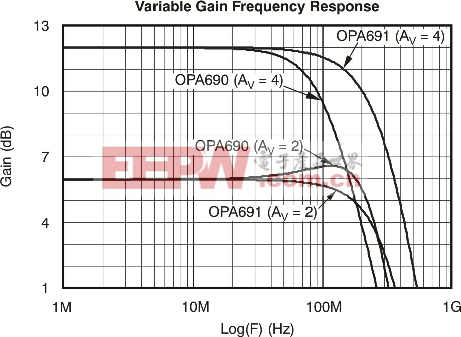
To compare,Figure 8shows the circuit of Figure 7 simulated at the gain extremes using both the CFB OPA691 and a very similar VFB device, the OPA690.
(Click to Enlarge Image)
Figure 8. Adjustable gain small-signal bandwidth comparison.
At a gain of +2 V/V (6 dB), both parts show about the same bandwidth (280 MHz) where the OPA691 is closer to a Butterworth response while the OPA690 is bit more peaked. Adjusted to a gain of +4 V/V (12 dB), the OPA691 still holds >220 MHz bandwidth while the OPA690 drops to around 100 MHz.
Most simple circuits not mentioned thus far can generally use either a VFB or CFB device. It is sometimes suggested that some of these circuits cannot be implemented using a CFB device; this claim is often incorrect. One example that demonstrates this is the differencing amplifier.
Example E
A single amplifier differential stage (sometimes called a 'differencing' amplifier) can use either VFB or CFB devices. The common-mode rejection ratio (CMRR) of a CFB implementation appears to be lower when compared to an equivalent VFB design. However, that CMRR is the effect of the buffer gain loss across the input stage and is quite repeatable for a particular CFB part number. It is possible to tune up the CMRR to a much higher dc level for a CFB differencing amplifier by slightly increasing the resistor to ground on the non-inverting input.
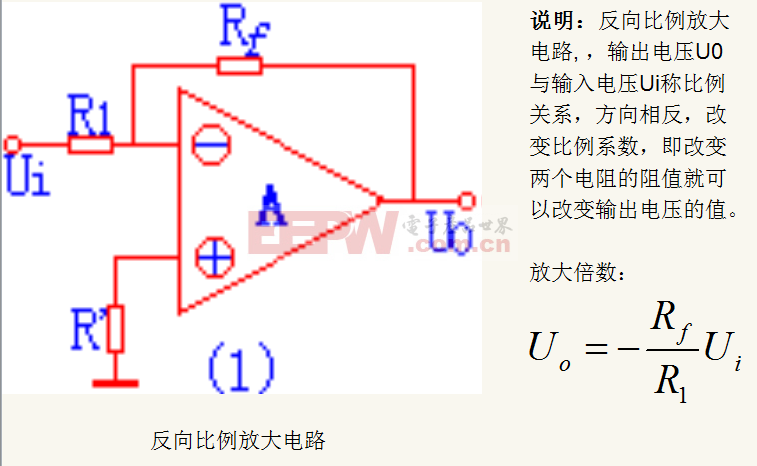
Figure 9shows a representative differencing amplifier using the very high slew rate, unity gain stable, VFB OPA690. Notice also that the resistors on the non-inverting side were adjusted down to achieve a matched input impedance for each source (if V1and V2are independent sources. SeeReference 1for an example of where they are not).


評(píng)論